Second Evaluation
No. 1 If the base resistor is very small, -the
-transistor will operate in the a. cutoff region b. active region c. saturation
region d. breakdown region
No. 2 If a transistor operates in the middle of the load
line, an increase in the base resistance will move the Q-point a. up b. down c.
nowhere d. off the load line
No. 3 The saturation point is approximately the same as
a. cutoff point b. lower end of the load line c. upper end of the load line
No. 4 When the collector resistance decrease in a base
biased circuit, the load line becomes a. more horizontal b. more vertical c.
fixed
No. 5 The first step in analyzing emitter biased circuits
is to find the a. base current b. emitter voltage c. emitter current d.
collector current
No. 6 If the emitter resistance decreases, the collector
voltage a. decreases b. stays the same c. increases d. breaks down the
transistor
No. 7 If the emitter resistance doubles in a VDB circuit,
the collector current will a. double b. drop in half c. remain the same d.
increase
No. 8
a) What is the emitter voltage?
b) The collector voltage?
c) Draw the load line, plot the Q-point!
d) Redesign the circuit to get the Q-point in the middle of the
load line.
Given: R1 = 12KW,
R2 = 3KW, RC = 3.2 KW, RE = 1KW,
VCE = 10V
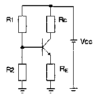
Figure