| Amplifier Teaching Aid (DED Philippinen, 86 p.) | |||||
| Lesson 6 - Transistor Biasing II | |||||
| Lesson Plan | |||||
| (introduction...) | |||||
| Transistor biasing II | |||||
| VDB analysis | |||||
| Worksheet No. 6 | |||||
|
| ||||||||||||||||||||||||||||||||||||||||||
Title: Transistor Biasing II
Objectives:
- Know the advantage of voltage divider
bias
- Able to analyse VDB circuits

Figure
Voltage Divider Bias
The most famous circuit based on -the prototype of emitter bias is called the voltage divider bias (VDB).
Recall the steps of analyzing the emitter bias circuit:
1. VE
2. IE
3.
IC
4. Voltage drop across RC
5. VC
6.
VCE
The three most important steps are:
1. IE
2. VC
3.
VCE

Fig. 6-1: Emitter biased
circuit
Problem: Sometimes the voltage from the VCC power supply is too large to apply directly at the base.
Solution:
- extra power supply for the base
- or
==> VDB
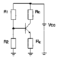
Fig. 6-2: VDB circuit
The voltage drop across R2 is applied directly to the base, which means:
V2 =
VB
1. step: find voltage drop across
R2
2. step: subtract 0.7V to get
VE
Design errors of 5% or less are acceptable, because of resistor tolerances.

Fig. 6-3: VDB example circuit
Find the base voltage:
Assumption: Base current is so small that it has no effect on the voltage divider.
5% error - > base current is 20 times smaller than the divider current.

VB = I * R2 = 0.82 mA * 2.2KW = 1.8V
VE = VB - VBE = 1.8V - 0.7V =
1.1V
VC = VCC -(RC * IC) = 10V - (3.6KW * 1.1 mA) = 6.04V
VCE = VC - VE = 6.04V - 1.1V = 4.94V
Checking the assumption:
5% error --> 
The current gain can vary from 30 to
300.
Even under the worst case condition the calculation is within the 5% limit, hence the assumption can be done.
Summary of Process and Formulas
|
Divider current |
|
|
Base voltage |
VB = I * R2 |
|
Emitter voltage |
VE = VB - VBE |
|
Emitter current |
|
|
Collector voltage |
VC = VCC - (IC * RC) |
|
Coll.- emitter voltage |
VCE = VC - VE |
HO: What will change if the emitter resistor increases to 2KW? (unchanged voltage divider)
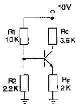
Fig. 6-4: VDB circuit
Solution:
I = 0.82 mA
VB = 1.8V
VE =
1.1V
VC = VCC - (RC * IC) = 8.02V
VCE = VC - VE = 6.92V
VDB Load-Line and Q-Point
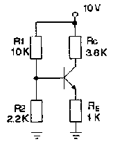
Fig. 6-5: VDB circuit
Saturation point:
Visualize short between collector and emitter
VRC = VCC - VE = 10V - 1.1V =
8.9V
- - > 
Cutoff point:
Visualize open between collector and emitter
- - > VCE (cut) = VCC - VE = 8.9V
Q-point:

VC = VCC - (IC * RC) = 10V - (1.1 mA * 1KW) = 6.04V
VCE = VC - VE = 6.04V - 1.1V = 4.94V
Now we plot these values and get the load line and the Q-point:

Fig. 6-6: Output curve with load
line and Q-point
The values VCC, RC, R1, and R2 are controlling saturation current and cutoff voltage. To move the Q-point is possible by varying the emitter resistance (RC).
Get the Q-point in the Middle of the Load Line
To set the Q-point is a important preparation as you will see later on.
Effect of RE:
RE too large -- > Q-point
moves into cutoff
RE too small --> Q-point moves into
saturation
Q - point in the middle of the load line:
Half the value of IC (sat) and redesign RE
IC (sat) = 2.47 mA ==> 1.23
mA
Look for the nearest standard value:
===> 910 W

Fig. 6-7: Output curve, Q-point in
the
middle
Figure
No. 1 What is -the emitter voltage? The collector voltage? Given: R1= 10k, R2= 2.2k, RC = 3.6k, RE = 1k, VCC = 25V
Draw the load-line, plot the Q point!
No. 2 What is the emitter voltage? The collector voltage?
Given: R1= 330k, R2= 100k, RC = 150k, RE = 51k, VCC = 10V
Draw the load-line, plot the Q point!
No. 3 What is the emitter voltage? The collector voltage? Given: R1 = 10k, R2 = 2.2k, RC = 2.7k, RE = 1k, VCC = 10V
Draw the load-line, plot the Q point!
Redesign the circuit to get the Q-point in the middle of the loadline!