
| Amplifier Teaching Aid (DED Philippinen, 86 p.) | |||||
| Lesson 8 - Small Signal Amplifier II | |||||
| Lesson Plan | |||||
| (introduction...) | |||||
| Signals in a CE amplifier | |||||
| Input impedance | |||||
| Impedance matching | |||||
| Handout No. 1 | |||||
| Worksheet No. 8 | |||||
|
| ||||||||||||||||||||||||||||||||||||||||||||||||||||||
Title: Small Signal Amplifier II
Objectives:
- Able to calculate the input
impedance
- Understand the purpose of impedance matching
Figure
One characteristic of the CE amplifier is the phase inversion.
See Handout No. 1 (let the students complete)
For a better understanding the different voltage signals are plotted in four graphs:
Graph 1: A small ac signal is applied at
the amplifier input.
Graph 2: The small ac signal is topping the biasing
dc.
Graph 3: The amplified and inverted ac signal is topping the biasing
dc.
Graph 4: The output capacitor C2 is blocking the dc, the
amplified inverted ac signal is applied at the
load.
Another important value to analyze is the input impedance of an amplifier circuit.
Recall the ac equivalent circuit in Lesson 7:
(see Fig. 8-1 on the next page)
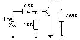
Fig. 8-1: AC equivalent circuit
RG is equal to the internal resistance of the signal source. Input impedance looking into the base:
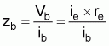
ie/ib is approximately equal to b:
zb = b * re
The input impedance of a amplifier stage is the combination of base impedance and biasing resistance:
zin = R1//R2//b * re
Ex: What is the input impedance in Fig. 8-1?
re = 22.7 W, b = 100
zin = 1.8 KW//22.7
W *
100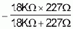
= 202 W
When you couple some amplifier stages or connect electronic appliances, the input/output impedance of every stage will effect the efficiency.
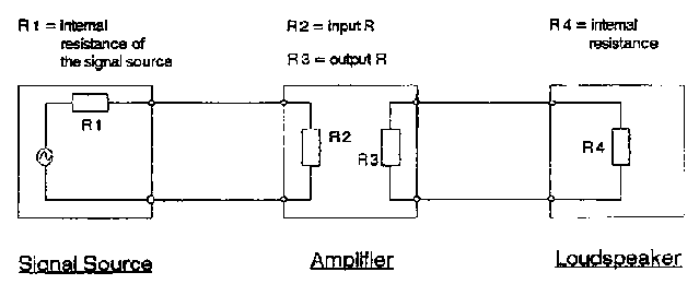
Fig. 8-2: Impedance matching
The internal resistance/impedance of the signal source (R1) and the loudspeaker (R4) is fixed. Only R2 and R3 can be designed to match the impedance.
Voltage optimum
Between signal source and amplifier it is important to transfer the highest possible voltage.
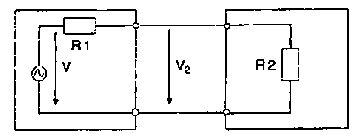
Fig. 8-3: Voltage optimum
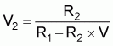
In order to get the highest, possible voltage (V2) let's try several values for R2.
Ex: V = 10V, R1 = 100 W
R2 = 0.1 *
R1 --- > 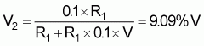
R2 = R1 ---
> 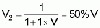
R2 = 10 * R1
--- > 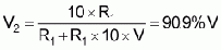
R2 = 100 * R1
--- > 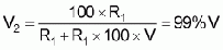
The input impedance of an amplifier should be much bigger than the internal resistance of the signal source.
Power Optimum
Between amplifier and loudspeaker it is most important to transfer the highest possible power.
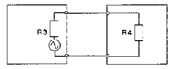
Fig. 8-4: Power optimum
Ex: Power in the load under different values of R4.
V = 10V, R3 = 8W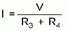 PL = R4 *
I2
PL = R4 *
I2
|
R4 = 16W |
I = 24W = 0.42A |
PL = 2.78W |
| | | |
|
R4 = 8W |
I = 16W = 0.63A |
PL = 3.125W |
| | | |
|
R4 = 4W |
I = 12W = 1.14A |
PL = 1 .03W |
Input impedance of the load and the output impedance of the amplifier should have the same value.
R3 = R4
Ri = RL
Figure
Figure
No. 1 a) The generator voltage doubles. What is the input impedance?
b) The generator resistance RG doubles. What is the input impedance?
No. 2 You like to connect a microphone (R = 100KW) to an amplifier. What should be the input impedance of the amplifier to get a voltage optimum?
Microphone output voltage Vout = 10 mV
No. 3 The output impedance of your amplifier is 6W. What kind of loudspeaker (4W or 8W) do you choose to get the best power transfer?