| Digital Teaching Aid (DED Philippinen, 86 p.) | |||||
| Data Processing Circuits - Lesson 9 | |||||
| Lesson Plan | |||||
| (introduction...) | |||||
| Introduction | |||||
| Multiplexer | |||||
| Demultiplexer | |||||
| Handout No. 3 | |||||
| Worksheet No. 9 | |||||
|
| ||||||||||||||||||||||||||||||||||||||||||||||||||||||
Titel: Data Processing Circuits
Objectives:
- Understand the principle of multiplexer and demultiplexer
- Able to use the multiplexer solution as design method
|
Time |
Method |
Topic |
Way |
Remark | |
| |
|
* Review Lesson 8 |
| | |
| | |
* Introduction |
| | |
| | |
* Multiplexer |
| | |
| | |
|
- Principle and logic circuit | | |
| | |
|
-The 74 150 |
| |
| | |
|
- Multiplexer design |
HO |
Handout No. 3 |
| |
|
* Demultiplexer |
| | |
| | |
|
- Principle and logic circuit | | |
| | |
|
-The 74 154 |
| |
| | |
* Review exercise |
WS |
Worksheet No. 9 | |
| |
S: Speech | |
B: Boardscript |
| |
Data Processing Circuits
Data processing circuits: Logic circuits that process binary data.
A multiplexer is a circuit with many inputs but only one output.
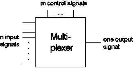
Fig. 9-1: Multiplexer
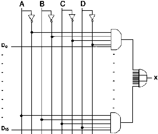
Fig. 9-2: Logic circuit, 16 to 1
multiplexer
A multiplexer is also called a data selector because the output bit depends on the input data that is selected. The input bits are labeled D0 to D15. Only one of them is transmitted to the output. Which one depends on the value of A B C D, the control input.
|
Ex: |
If A B C D = 0 0 0 0 |
| |
the output will be: |
| |
® Y = D0 |
| |
So the input bit DO is selected. |
| |
Or if A B C D = 1 1 1 1 |
| |
® Y = D15 |
The control nibble (nibble = 4 bit) A B C D determines which of the input data bits is transmitted to the output.
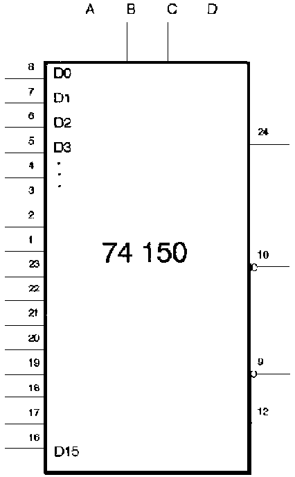
The 74 150
The TTL device 74 150 is a 16 to 1 multiplexer with inverted output. (see Fig. 9-2, instead of a OR gate, a NOR gate is used to invert the output)
Ex: When A B C D = 1 0 0 1

Fig. 9-3: Pinout diagram, 74150 16
to 1 multiplexer
Pin 9 (STROBE) is an input signal that disables or enables the multiplexer.
Fig. 9-4: Truth table, 74 150
|
STROBE |
A |
B |
C |
D |
X |
|
L |
0 |
0 |
0 |
0 |
|
|
L |
0 |
0 |
0 |
1 |
|
|
L |
0 |
0 |
1 |
0 |
|
|
L |
0 |
0 |
1 |
1 |
|
|
L |
0 |
1 |
0 |
0 |
|
|
L |
0 |
1 |
0 |
1 |
|
|
L |
0 |
1 |
1 |
0 |
|
|
L |
0 |
1 |
1 |
1 |
|
|
L |
1 |
0 |
0 |
0 |
|
|
L |
1 |
0 |
0 |
1 |
|
|
L |
1 |
0 |
1 |
0 |
|
|
L |
1 |
0 |
1 |
1 |
|
|
L |
1 |
1 |
0 |
0 |
|
|
L |
1 |
1 |
0 |
1 |
|
|
L |
1 |
1 |
1 |
0 |
|
|
L |
1 |
1 |
1 |
1 |
|
|
H |
X |
X |
X |
X |
H |
With high STROBE the value of A B C D doesn't matter, the output will allways be high.
Multiplexer Logic (Multiplexer Design)
The starting point for digital design is usually the truth table. We already discussed two standard methods for implementing a truth table:
- sum of products method
- product of sums method
Now we are ready for the third method:
- the multiplexer solution
The following example explains the multiplexer solution. (Please refer to Handout No. 3)
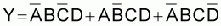
Ex: First we have to complement each output in the truth table (Y), that will be the corresponding data input for the multiplexer:
|
Y = 1 ® 0 ® D0 |
|
Y = 0 ® 1 ® D1 |
|
Y = 1 ® 0 ® D2 |
|
Y = 1 ® 0 ® D3 |
|
. |
|
. |
|
. |
|
and so on for every value of Y |
Next, wire the data inputs of the 74 150, so that they equal the foregoing values:
|
D0 ® grounded |
|
D1 ® connected to 5V |
|
D2 ® grounded |
|
D3 ® grounded |
|
. |
|
. |
|
. |
|
D15 ® grounded |
Check the circuit:
When A B C D = 0 0 0 0® D0 is the selected input since D0 is low. Y is high
Please check also the remaining input possibilities!
Universal logic circuit
The 74 150 can be used as a design solution for any 4 variable truth table.
A demultiplexer is a circuit with only one input but many outputs.
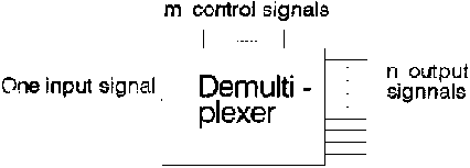
Fig. 9-5: Demultiplexer
By applying control signals, we can steer the input signal to one of the output lines.
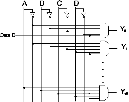
Fig. 9-6: Logic circuit, 1 to 16
demultiplexer
The 74 154
The 74 154 is a 1 to 16 demultiplexer, with active low STROBE and DATA input.
Fig. 9-7: Truth table, 74 154 1 to 16 demultiplexer
|
STROBE |
DATA |
A |
B |
C |
D |
Y |
|
L |
L |
0 |
0 |
0 |
0 |
Y0 |
|
L |
L |
0 |
0 |
0 |
1 |
Y1 |
|
L |
L |
0 |
0 |
1 |
0 |
Y2 |
|
L |
L |
0 |
0 |
1 |
1 |
Y3 |
|
L |
L |
0 |
1 |
0 |
0 |
Y4 |
|
L |
L |
0 |
1 |
0 |
1 |
Y5 |
|
L |
L |
0 |
1 |
1 |
0 |
Y6 |
|
L |
L |
0 |
1 |
1 |
1 |
Y7 |
|
L |
L |
1 |
0 |
0 |
0 |
Y8 |
|
L |
L |
1 |
0 |
0 |
1 |
Y9 |
|
L |
L |
1 |
0 |
1 |
0 |
Y10 |
|
L |
L |
1 |
0 |
1 |
1 |
Y11 |
|
L |
L |
1 |
1 |
0 |
0 |
Y12 |
|
L |
L |
1 |
1 |
0 |
1 |
Y13 |
|
L |
L |
1 |
1 |
1 |
0 |
Y14 |
|
L |
L |
1 |
1 |
1 |
1 |
Y15 |
|
L |
H |
X |
X |
X |
X |
H |
|
H |
L |
X |
X |
X |
X |
H |
|
H |
H |
X |
X |
X |
X |
H |
Example for Multiplexer Solution
Problem: Design a logic circuit for the problem which is given through the truth table below. Use a 74150 to implement this table:
|
A |
B |
C |
D |
Y |
|
0 |
0 |
0 |
0 |
1 |
|
0 |
0 |
0 |
1 |
0 |
|
0 |
0 |
1 |
0 |
1 |
|
0 |
0 |
1 |
1 |
1 |
|
0 |
1 |
0 |
0 |
1 |
|
0 |
1 |
0 |
1 |
1 |
|
0 |
1 |
1 |
0 |
0 |
|
0 |
1 |
1 |
1 |
0 |
|
1 |
0 |
0 |
0 |
1 |
|
1 |
0 |
0 |
1 |
1 |
|
1 |
0 |
1 |
0 |
1 |
|
1 |
0 |
1 |
1 |
1 |
|
1 |
1 |
0 |
0 |
1 |
|
1 |
1 |
0 |
1 |
1 |
|
1 |
1 |
1 |
0 |
0 |
|
1 |
1 |
1 |
1 |
1 |
Solution: Complement each Y output to get the corresponding data input:
D0 = 1 = 0Dl = 0 =
D2 =
D3 =
D
D
D
D
D
D
D
D
D
D
D
D15=
Connect: the chip in response to the list of corresponding data inputs:
Figure
Universal Logic Circuit
This circuit is an example of multiplexer logic. You ................. an input data pin when the corresponding output is ............... in the truth table.
You connect an input data pin to .............................. if the corresponding output is..................... in the truth table.
No. 1 In Fig. 9-1, if
a) A B C D = 0 1 1 0
b) A B C D = 1 0 0 1
c) A B C D = 1 1 0 1
what does Y equal?
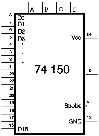
Fig. 9-1: 74 150, 16 to 1 multiplexer
No. 2 Show how to connect a 74150 (use Fig. 9-1) to implement the following Boolean equation:
No. 3 Draw a circuit with two 74150's that has the truth table like the following one:
|
A |
B |
C |
D |
Y1 |
Y2 |
|
0 |
0 |
0 |
0 |
0 |
0 |
|
0 |
0 |
0 |
1 |
1 |
0 |
|
0 |
0 |
1 |
0 |
0 |
0 |
|
0 |
0 |
1 |
1 |
0 |
1 |
|
0 |
1 |
0 |
0 |
0 |
0 |
|
0 |
1 |
0 |
1 |
1 |
1 |
|
0 |
1 |
1 |
0 |
1 |
1 |
|
0 |
1 |
1 |
1 |
1 |
1 |
|
1 |
0 |
0 |
0 |
0 |
1 |
|
1 |
0 |
0 |
1 |
1 |
0 |
|
1 |
0 |
1 |
0 |
1 |
0 |
|
1 |
0 |
1 |
1 |
1 |
0 |
|
1 |
1 |
0 |
0 |
0 |
0 |
|
1 |
1 |
0 |
1 |
1 |
0 |
|
1 |
1 |
1 |
0 |
1 |
1 |
|
1 |
1 |
1 |
1 |
0 |
0 |