
| Digital Teaching Aid (DED Philippinen, 86 p.) | |||||
| Flip-Flops - Lesson 7 | |||||
| Lesson Plan | |||||
| (introduction...) | |||||
| Introduction | |||||
| RS Flip-Flops | |||||
| D - Flip-Flop (D-FF) | |||||
| JK Flip-Flop (JK-FF) | |||||
| Worksheet No. 7 | |||||
|
| ||||||||||||||||||||||||||||||||||||||||||||||||||||||
Titel: Flip-Flops
Objectives:
- Understand the Flip-Flop principle
- Know the three basic Flip-Flops (RS, D, JK)
- Able to analyze timing diagrams
|
Time |
Method |
Topic |
Way |
Remark |
| |
|
* Review Lesson 6 |
| |
| | |
* Introduction |
| |
| | |
* RS Flip-Flops |
| |
| | |
* Clocked RS-FF |
| |
| | |
* Timing diagram |
| |
| | |
* D-FF | | |
| | |
* FF switching time |
| |
| | |
* JK-FF | |
|
| | |
* JK-MS-FF | |
|
| | |
* Review exercise |
|
Worksheet No. 7 |
| |
S: Speech | |
B: Boardscript | |
Flip-Flops
Sometimes there is a need of digital devices or circuits whose output will remain unchanged, once set, even if there is a change in input.
A Flip-Flop is a bistable electronic circuit that has two stable states.
Þ Output is either 0 or 5V dc
The Flip-Flop can be regarded as a memory device. It can be used to store one binary digit at the output.
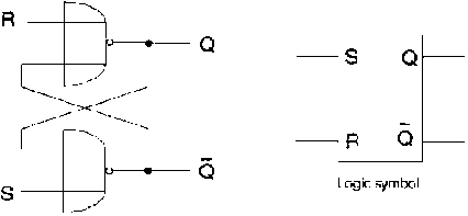
Fig. 7-1: RS Flip-Flop, logic
circuit and device symbol
HO: What is the truth table for the circuit above?
Solution:
Fig. 7-2: Truth table, RS Flip-Flop
|
R |
S |
Q |
Action |
|
0 |
0 |
Last value |
No change |
|
0 |
1 |
1 |
Set |
|
1 |
0 |
0 |
Reset |
|
1 |
1 |
? |
Forbidden |
If both inputs (R, S) are high at once, the output can not be determined before; therefore, it is a forbidden state.
Ex: Create a RS Flip-Flop with NAND gates.
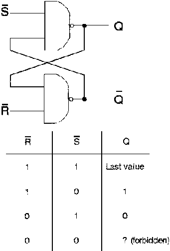
Fig. 7-3: RS Flip-Flop with NAND
gates
Note: The inputs (R, S) are indicated with an overbar so they are inverted.
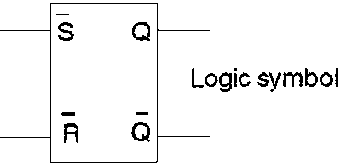
Fig. 7-4: Logic symbol, RS
Flip-Flop with inverted inputs
Clocked RS Flip-Flop
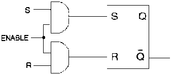
Fig. 7-5: Clocked RS Flip-Flop
This Flip-Flop ca be enabled or disabled.
ENABLE ® low: R and S will have no effect on the output
ENABLE ® high: R and S inputs will be directly transmitted to the output
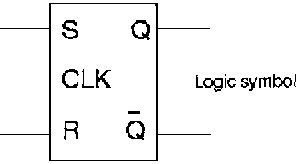
Fig. 7-6: Logic symbol, Clocked RS
Flip-Flop
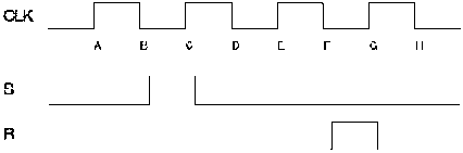
Timing diagram
A timing diagram is a drawing to determine the time dependent actions of logic devices.
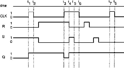
Fig. 7-7: Timing diagram of a
clocked RS Flip-Flop
Fig. 7-7 shows that the inputs (R, S) effect the output (Q) only when the clock signal (CLK) is high.
RS Flip-Flop application: Bounce free switch
The generation of two signals to drive a Flip-Flop is a disadvantage in many applications. This has led to the D-FF, a circuit that needs only a single data input.
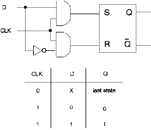
Fig. 7-8: D Flip-Flop, logic
circuit and truth table
CLK ® low: D can change without effect on the output
CLK ® high: Q is forced to equal the value of D
Ex: Create a 4 bit data memory with D-latches (D-FF).
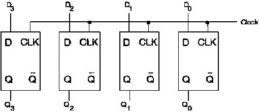
Fig. 7-9: Data storage with
D-FF
In Fig. 7-9, when the clock goes high, input data is loaded into the Flip-Flops and appears at the output.
Suppose the data input is:
D3 D2 D1 D0 = 1 0 1 0
When the clock goes high this 4 bit word is loaded into the D-latches, resulting in an output of:
Q3 Q2 Q1 Q0 = 1 0 1 0
Flip-Flop switching time
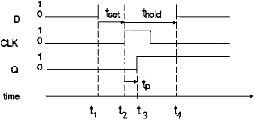
Fig. 7-10: Timing diagram, FF
switching time
|
tset: |
Minimum of time that the date bit must be present before the clock edge hits (because of stray capacitance) |
|
thold: |
The data bit has to be hold long enough for the internal transistors to switch. |
|
tp: |
Switching time, diodes and transistors cannot switch states immediately. (some nanoseconds) |
Flip - Flops can be used to build counters, JK-FF are the ideal elements for that purpose.
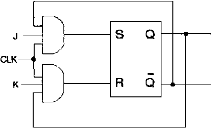
Fig. 7-11: JK-FF, logic circuit
Ex: What is the truth table for the circuit above?
Fig. 7-12: Truth table, JK-FF
|
CLK |
J |
K |
Q |
|
X |
0 |
0 |
last state |
|
|
0 |
1 |
0 |
|
|
1 |
0 |
1 |
|
|
1 |
1 |
toggle |
|
J and K ® low: |
Both AND gates are disabled, clock pulses have no effect. Q retains its last value. |
|
J ® low, K ® high: |
The upper gate is disabled, only reset is possible (unless Q is already reset). |
|
J ® high, K ® low: |
The lower gate is disabled, only set is possible (unless Q is already high). |
|
J and K ® high: |
Set or reset is possible, the Flip-Flop will “toggle” on the next positive clock edge. Toggle means to switch to the opposite state. |

Fig. 7-13: JK-FF's, logic
symbols
Preset (PR) and Clear (CLR) are input signals to get a definite start point.
JK Master-Slave FF (JK-MS-FF)
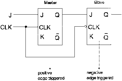
Fig. 7-14: JK-MS-FF, logic
circuit
Regardless what the master does, the slave copies it. The slave copies the master on the negative clock edge. This circuit provides a way to avoid racing.
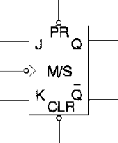
Fig. 7-15: JK-MS-FF, logic
symbol
Available as TTL device: 74 LS 76
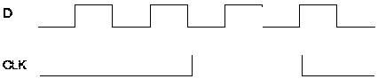
No. 1 A JK master slave FF has its inputs tied to + 5V, and a series of pulses are applied to its CLK input Describe the Q output.

Figure
No. 2 The signal drives a clocked RS - FF. If Q is low before point A in time: At what point does Q becomes a 1? What does Q reset to 0?
Figure
No. 3 Use the information in the preceding problem and draw the waveform Q.
No. 4 The signal drives a D-FF. What is the value of stored in the FF after the clock pulse is over?
Figure
No. 5 A normal JK-FF, J = K = 1. A 1 MHz is applied to the CLK input it has a propagation delay tp of 50 ns. Draw the input squarewave and the out put expected at Q. Be sure to show the propagation delay time.