Back to Home
Page of CD3WD Project or Back to list of CD3WD Publications
 |  |  | Renewable Energy Technologies: A Review of the Status and Costs of Selected Technologies (WB, 1994, 184 p.) |  |  | 4 Photovoltaics | |  | Introduction | | | Photovoltaic manufacturing and technology | | | (introduction...) | | | Efficiency | | | Crystalline sillicon solar cells (''Thick'' Film) | | | Thin-film solar cells | | | Concentrator solar cells | | | Environmental effects | | | The cost of photovoltaic power | | | Costs in detail | | | (introduction...) | | | Modules costs | | | Balance-of-system costs | | | Cost of photovoltaic electricity | | | The future of photovoltaics |
|
Renewable Energy Technologies: A Review of the Status and Costs of Selected Technologies (WB, 1994, 184 p.)
4 Photovoltaics
Introduction
The previous two chapters have described the conversion of solar
energy to electricity through either the combustion of the product of
photosynthesis to generate heat energy or the use of direct solar energy to heat
a fluid and drive a turbo generator. This chapter describes a completely
different way of generating electricity from sunlight: converting light energy
directly to electrical energy using photovoltaic (PV) devices.
Photovoltaic devices work by using an effect first discovered in
1839 by Becquerel but not used in commercial applications until the 1950s (see
Annex 7; "The Photovoltaic Effect"}. These early applications were in the space
industry, and development of photovoltaics for terrestrial use began only in the
1970s. In the last two decades, however, development of photovoltaics has been
nothing short of remarkable. The technology is described briefly and then
discussed in relation to costs.
The recent and rapid advances in photovoltaic technology have
been driven by technical innovations and contributions from several distinct
scientific disciplines, including materials sciences, solid-state
(semiconductor) physics, and optics. The technology is also notable for the
variety of approaches being pursued by different laboratories and manufacturers,
resulting in a healthy competition of ideas among innovators and in significant
progress in the laboratory and in manufacturing.
The world market for photovoltaics was 57.9 MW in 1992, having
increased from less than 1 MW in 1978 (Figure 4.1). Current uses of photovoltaic
modules include the following:
· Lighting (e.g.,
street lights, highway signs, parking lots, health clinics, and homes).
· Electricity for facilities in
remote locations (e.g., refrigeration in remote health clinics or homes).
· Communications (e.g.,
telephones, radio communications, and emergency call boxes).
· Water pumping (e.g., village
water supply, irrigation and drainage).
· Warning signals (e.g.,
navigational beacons such as buoys and lighthouses, audible signals, railroad
signals, and aircraft warning beacons).
· Monitoring at remote sites
(e.g., seismic recording, meteorological information, structural conditions and
scientific research).
· Cathodic protection (e.g.,
preventing corrosion of pipelines, bridges, and buildings).
· Battery charging for
vehicles.

Figure 4.1. Global Photovoltaic
Market,
1976-1992
Photovoltaic manufacturing and technology
Photovoltaic modules are made from a number of materials and
fabricated in a variety of different designs. An understanding of the designs
and the direction of further improvements requires some knowledge of the
principle of the Photovoltaic effect (Annex 7 explains the effect for
single-crystal silicon; the principle is the same for other semiconductor
materials). In brief, when sunlight shines on these materials, it frees
electrons from fixed sites. The wavelength of the sunlight absorbed depends on
the "band gap" of the material. The materials are designed so that the electrons
cannot return to these sites easily except by flowing through an external
circuit, thus generating a current. A typical solar cell consists of a layer of
semiconductor material sandwiched between conducting top and bottom layers.
Photovoltaic modules are made up of several interconnecting solar cells, as the
individual PV cells do not provide much power. PV modules are generally less
than 1m2 in size and deliver between 50 and 150 W of electric power Thornton and
Brown 1992). The whole is encapsulated in a clear, waterproof coating to protect
the cells from the environment. Modules can be further interconnected to form
arrays. These are generally of two types: "non-tracking" arrays that remain in a
fixed position and "tracking" arrays that follow the sun's movement across the
sly. The latter are more complex and more expensive, but they can optimize the
system's performance (Thornton and Brown
1992).
Efficiency
The efficiency of a solar cell is measured by the percentage of
solar energy incident on the cell that is converted to electrical energy. This
percentage varies with cell materials and design. Strategies for increasing cell
efficiencies include the following (Kelly 1993; U.S. DOE 1991):
· The surface of the
cell is textured with small, pyramidal shapes that allow light reflected off the
surface to reflect back into the cell so that it can be absorbed.
· Electrical contacts on the
front of the cell are designed so that the maximum amount of light can reach the
semiconductor (e.g., top contacts can either be transparent or in the form of a
metal grid with thin, conductive "fingers").
· The amount of light that
passes through the material without colliding with an electron can be minimized
by selecting materials that are good light absorbers.
· Light-generated electrons and
holes recombine easily if they reach a flaw or an impurity in the crystal. These
flaws are minimized in polycrystalline or amorphous silicon by inaction with
hydrogen.
· Electrical resistance within
the cell can be minimized by good cell design.
· Stacking of cells with
different band gaps can ensure that a broader range of the solar spectrum is
captured, despite restrictions imposed by the band gaps of individual cells.
These stacked configurations are called multifunctional devices.
A number of approaches are therefore available for increasing
the efficiency of photovoltaic cells. However, there are trade-offs between
increases in efficiency and resulting increases in costs. For example, gallium
arsenide has a near-ideal band gap for single-junction devices, is a
particularly good light absorber. But its cost is considerably greater than that
of silicon. Hence, gallium arsenide has yet to penetrate the terrestrial market
significantly. Similarly, although single-crystal silicon modules have achieved
higher efficiencies (10 to 13 percent) than amorphous silicon modules
(stabilized efficiency of 3 to 5 percent), the manufacturing cost of the latter
is much lower. Thus, despite their lower efficiency, the amorphous silicon
modules have captured a third of the world market.
Annex 8 summarizes data relating to photovoltaics from a large
number of sources. Annex 9 shows only the efficiency data extracted from Annex
8, with the exception of items 117 to 128, 168 to 172, 225, and 267. These have
not been used because in items 117 to 128 and 168 to 172 it is not clear whether
the values are for cells or modules. In the case of items 225 and 267, the date
for these projected efficiency values is not given. The data have then been
plotted in several graphs according to semiconductor material (figures 4.2 to
4.6). Figure 4.7 shows efficiencies of cells and modules where the semiconductor
material has not been specified.
The following points need to be noted with regard to
interpretation of these data and estimates:
Efficiencies quoted for years after 1992 are projected; those
quoted up to and including 1992 are actual values.
· Cell efficiencies,
experimental efficiencies, and laboratory efficiencies have been taken to mean
efficiency values obtained in the laboratory for individual cells.
· Module efficiencies and
commercial module efficiencies have all been assumed to be field module
efficiencies. Distinctions between prototype and field modules have been noted,
if they have been specified by the source. The latter tend to be lower because
of the effects of dust and other factors experienced in the field.
· Sub-module efficiencies. where
specified as such (i.e., for smaller modules), have been noted as prototype
module efficiencies.
· Light-induced degradation
occurs when amorphous silicon devices are operated, thus reducing the initial
efficiency to a stabilized value after a few months of operation (see the
explanation in the section on thin-film solar cells). The efficiencies have been
noted as such in Figure 4.3.
· Efficiency also varies with
manufacturing method. For example, a single-crystal silicon cell manufactured by
the dendritic web method differs in efficiency from the same cell made by the
Czochralski method (see the section on "thick-film" cells).
· The lines drawn on the graphs
are only to aid the reader in visualizing trends and are not based on actual
efficiency values.

Figure 4.2. Efficiencies of
Crystalline Silicon Calls and Modules

Figure 4.3. Efficiencies of Amorphous
Silicon Cells and Modules

Figure 4.4. Efficiencies of Cadmium
Telluride (CdTe) Cells and Modules

Figure 4.5. Efficiencies of Copper
Indium Diseienide (CIS) Cells and Modules

Figure 4.6. Efficiencies of Gallium
Arsenide (GaAs) Cells and Modules
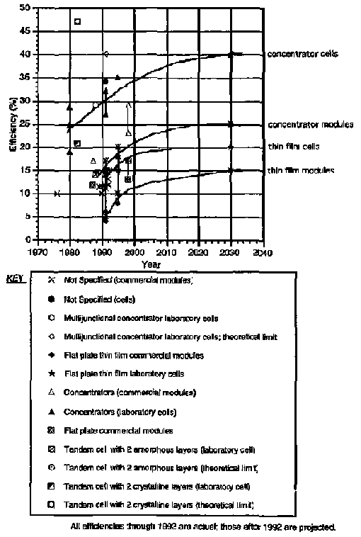
Figure 4.7. Efficiencies of
Photovoltaic Cells and Modules
The following general conclusions may be drawn from the graphs:
· Efficiencies
increased in the last few years. For example, efficiencies of crystalline
silicon modules have increased from 7 to 8 percent in 1976 to 10 to 13 percent
in 1992 (Figure 4.2); for cadmium telluride thin-film prototype modules, from 5
percent in 1986 to 10 percent in 1992 (Figure 4.4); and for CIS thin-film
prototype modules, from 5 percent in 1986 to 11 percent in 1992 (Figure 4.5).
· Cell efficiencies are greater
than module efficiencies. The time lag is not only different for different types
of photovoltaic module but is also different for different time periods. For
example, in the case of crystalline silicon, the time lag appears to have been
about five years between 1980 and 1985; but modules are not expected to reach
efficiencies of 17 percent (achieved by cells in 1984) till 2030 (Figure 4.2).
· Concentrator and
multifunctional cells are more efficient than monojunctional cells operating
under regular light. For example, amorphous silicon monojunctional cells have
stabilized efficiencies of 6 percent, whereas the multifunctional cells have
stabilized efficiencies of 10 percent (Figure 4.3). This is also partly because
stacking reduces light-induced cell degradation. Crystalline gallium arsenide
cells under regular light have exhibited efficiencies of 25 percent, whereas the
concentrator cells have efficiencies of 27 to 30 percent (Figure 4.6).
Similarly, under regular light, crystalline silicon cells have efficiencies of
22 to 24 percent, whereas the concentrator cells have achieved efficiencies of
28 percent (Figure 4.2).
The scope for further efficiency improvements is significant.
Practical theoretical efficiencies for monojunctional cells, under regular
light, are about 30 to 33 percent for crystalline silicon, 27 to 28 percent for
amorphous silicon, 27 to 28 percent for thin-film cadrnium telluride, 23.5
percent for thin-film copper indium diselenide, and 33 percent for crystalline
gallium arsenide. Theoretical values are given in the literature of 40 percent
for multifunctional concentrator cells, 29 percent for a tandem cell with two
amorphous layers, 47 percent for a tandem cell with two crystaline layers, and
42 percent for mechanically stacked amorphous silicon and copper indium
diselenide.
Details in Figures 4.2 to 4.6 are discussed further in the
following sections.
The scale of the variety in solar cell manufacture and design is
illustrated by Figure 4.8 and can be seen in the charts on efficiency (Figures
4.2 to 4.7). Many devices are also being investigated and manufactured, and
allowing for these makes the total range of approaches being followed by
scientists and engineers in research laboratories and in commercial companies
even larger. As noted, no dominant approach has emerged, and the competition
among ideas is intense and healthy. Some common types of solar cells are
described in more detail below.

Figure 4.8. Variety In Photovoltaic
Cells and Manufacturing
Processes
Crystalline sillicon solar cells (''Thick'' Film)
Single-Crystal Sllicon. In 1980, single-crystal silicon cells
accounted for 90 percent of commercial PV cells. In 1990, they were only 35
percent of the total world market, with amorphous silicon at 31 percent and
semicrystalline silicon at 33 percent.
The cell contains a wafer cut from a single crystal of silicon.
The raw material is waste silicon from the semiconductor industry, which PV
manufacturers purchase at a reduced price (Remy and Durand 1992; Kelly 1993).
The silicon is melted and regrown into large crystals. The two most established
methods for this are the Czochralski method and the floating-zone technique. In
the former, a seed crystal is dipped into a reservoir of molten silicon and
slowly drawn from it to form a large cylindrical crystal; in the latter, a rod
of polysilicon is placed above a seed crystal, and movable heating coils are
used to melt the polysilicon rod at the interface, allowing it to resolidify as
a single crystal (see U.S. DOE 1991; Green 1993 for descriptions of the
methods). These crystals are then sliced into wafers.
This process results in the waste of much silicon, as the
cylindrical ingots are much larger in diameter than the required wafers.
Alternative methods that minimize waste and cut manufacturing costs, such as the
use of thinner saws to slice the wafers or direct growth of thin crystalline
sheets or ribbons of silicon are being investigated actively to reduce
manufacturing costs (see Green 1993; Carlson, 1990; and U.S. DOE 1991). These
methods include (a) the dendritic web approach, in which two dendrites a few
centimeters apart are drawn from the melt, trapping a thin sheet of molten
silicon in between, which solidifies; (b) the edge-defined film-fed (EFG) growth
method, in which molten silicon moves by capillary action between two faces of a
graphite die and a thin sheet is drawn from the top of the die; and (c) the
S-Web approach, in which a carbon web is coated with silicon as it is drawn
through a silicon melt.
One potential problem in PV manufacture is that the quantity of
silicon that will be required in the near future, as the market of photovoltaics
increases, is in excess of the current silicon waste produced by the
semiconductor industry, indicating that silicon production specifically for the
PV industry will be required. Silicon is the second most abundant element on
Earth, but it is present in the form of silica (silicon and oxygen) and
silicates (compounds of silicon, oxygen, metals, and possibly hydrogen). Silica
is processed into silicon, which is then refined. The silicon used in PV
manufacture can be less pure than that needed for semiconductors, but current
production procedures are expensive, and some work is being carried out to
develop new, low-cost methods for silicon production (U.S. DOE 1991; Green
1993). However, some authorities feel that this matter merits more attention
(Remy and Durand 1992; and Pistella 1992).
Efficiencies of single-crystal cells and modules are shown in
Figure 4.2. Currently, efficiencies of experimental cells are 22 to 24 percent,
and those of modules (based on field experience) are 11 to 13 percent.
Theoretical efficiencies for single-crystal silicon are 30 to 33 percent. A
multifunction of a mechanically stacked gallium arsenide cell on top of a
singlecrystal silicon cell is reported to have achieved 31 percent efficiency
under concentrated light in 1988 (see the section on solar concentrator cells;
U.S. DOE 1991).
Polycrystalline Silicon Polycrystalline silicon is also used for
PV cell manufacture. Here, the semiconductor material consists of many crystals
of silicon. The associated problems in terms of increased electrical resistance
caused by the electrons and holes meeting at cell boundaries and recombining are
overcome to a certain extent by reaction with hydrogen or oxygen to fill the
broken bonds at the grain boundaries or by heating and cooling the material so
that the crystals are enlarged further, thus reducing the number of cell
boundaries within the material (U.S. DOE 1991). Nevertheless, polycrystalline
cells are less efficient than singlecrystal silicon cells, with efficiencies of
8 to 9 percent for field modules and 18 percent for experimental cells (Figure
4.2).
However, the corresponding decrease in efficiency is compensated
to a certain extent by the lower cost of manufacture for these cells. Silicon
wafers are manufactured by cooling molten silicon in a crucible in a controlled
manner to form an ingot, which is then cut into smaller blocks and sliced into
wafers. Methods for producing thin films of silicon on different supports (such
as ceramic and steel) are also being investigated, with the intention of
reducing costs, as less silicon is use d in these
devices.
Thin-film solar cells
Thin films require substantially less active material than
single-crystal silicon. Films are typically of thicknesses 0.001 to 0.002 mm, as
opposed to about 0.3 mm for a typical thickfilm single crystal or
polycrystalline silicon cell (Thornton and Brown 1992). Manufacturing techniques
are also different, with thin layers of different materials being deposited
sequentially, in a continuous process, on top of each other on a substrate
(usually glass), from the back electrical contact (usually a thin layer of
transparent oxide) to the semiconductor material to the antireflective coating
to the front electrical contact, to eventually make up the module. The sheets
are then divided into individual (interconnected) cells by scoring with a laser
beam (U.S. DOE 1991). The manufacturing procedures are potentially much less
costly than growing single crystals, because in addition to using as little as 1
percent of active material compared with the latter, they hold great potential
for low-cost, automated, large-scale production (Kelly 1993; Zwiebel and Barnett
1993; U.S. DOE 1991).
Amorphous Silicon. Amorphous silicon (a glassy alloy of silicon
and about 10 percent hydrogen) was regarded as an insulator until 1974, when it
was demonstrated to be a semiconducting material. By '990, amorphous silicon PV
cells formed 31 to 32 percent of the world market for PVs (Carlson and Wagner
1993; U.S. DOE 1991). The active cell has slightly different construction, with
a neutral layer of amorphous silicon (the "i" or intrinsic layer) present
between the thin, highly doped, top p-layer and the bottom e-layer. It is here
that the electron-hole pairs are generated, thus facilitating their movement, as
electrons and holes are far less mobile in amorphous silicon than crystalline
silicon, and doping worsens this situation (U.S. DOE 1991).
The first cell had an initial efficiency of I percent in 1974,
which decreased on exposure to light to as little as 0.25 to 0.5 percent
(Carlson and Wagner 1993). Efficiencies for amorphous silicon cells are shown in
Figure 4.3. It is worth noting that a decrease of 10 to 20 percent from the
initial efficiency occurs in the first few months of use because of
light-induced degradation of the amorphous silicon (Carlson and Wagner 1993;
U.S. DOE 1991). Currently, stabilized monojunctional experimental cell
efficiencies are about 6 percent, and stabilized field module efficiencies are
in the range of 3 to 5 percent. Estimates in the literature for theoretical
efficiency limits for single-junction amorphous silicon cells are 22 percent and
27 to 28 percent (Cody and Tiedje 1992 for the lower value; Kelly 1993 for the
higher).
Multijunctional devices, with higher efficiencies, have also
been developed for amorphous silicon. Use of this configuration not only
improves the overall efficiency of the cell but, in the case of amorphous
silicon, results in a further increase in the overall efficiency of the
individual cells because the thinner layers of material result in less
light-induced degradation (International Energy Agency 1987; U.S. DOE 1991). The
band gap of amorphous silicon can be altered by the formation of alloys with
germanium, carbon, tin, and nitrogen. Thus, typically three amorphous silicon
cells with different band gaps are stacked to form a multifunctional cell.
Multijunctional amorphous silicon cells have stabilized laboratory efficiencies
of 10 percent (6 percent for field modules; Figure 4.3). An amorphous silicon
cell has also been stacked on top of a CIS cell, achieving initial efficiencies
in the laboratory of 16 percent and 12 percent for submodules (Figure 4.5).
The lower efficiency of the modules relative to single-crystal
silicon is balanced by their significantly lower cost per unit area due to the
smaller quantity of active material needed because of its high absorptivity (40
percent greater than single-crystal silicon), as well as the lower temperatures
required for production and the use of low-cost substrates for deposition of the
active material (U.S. DOE 1991).
Cadmium Telluride (CdTe). Efficiencies of cadmium
telluride-based laboratory PV cells are in the range of 12 to 16 percent, with
prototype modules having efficiencies of 8 to 10 percent (see Figure 4.4.).
Theoretical efficiencies are estimated at 27 to 28 percent. CdTe cells do not
show the light-induced instability found in amorphous silicon. Two cell designs
are predominant. In the first, CdTe forms the p-layer, and cadmium sulfide forms
the elayer. However, CdTe is highly resistive when doped, and this problem has
been circumvented in another design that makes CdTe into an intrinsic layer,
sandwiched between pzinc telluride and e-cadmium sulfide (U.S. DOE 1991).
Cadmium telluride-based cells are about to be commercialized, after benefiting
from the experience of research in the late 1970s and early 1980s, when several
companies unsuccessfully attempted to commercialize these cells (Zweibel and
Barnett 1993).
Copper Indium Diselenide (CIS). Efficiencies of copper indium
diselenide PV cells are in the range of 14 to 15 percent, with prototype modules
demonstrating efficiencies of 11 percent (see in Figure 4.5). The theoretical
efficiency for single-junction thin-film CIS cells is estimated as 23.5 percent
by one source (Kelly 1993). These cells consist of a p-layer of CIS and an
e-layer of cadmium sulfide (U.S. DOE 1991). Copper indium diselenide is also
both being used in various designs of multijunctional cells (U.S. DOE 1991). An
amorphous silicon cell has also been stacked on top of a CIS cell, achieving
initial efficiencies in the laboratory of 16 percent (12 percent for submodules;
Figure 4.5).
CIS not only has high absorptivity, absorbing as much as 99
percent of the incident light, but also displays good stability with regard to
light degradation (U.S. DOE 1991). CIS modules are amenable to low-cost,
large-scale manufacture and are seen by many as the "model" thin film. It is
worth noting, however, that indium supply may become an issue if CIS modules
enter large-scale production. Indium is thought to be as abundant as silver, but
current supply capacity cannot meet heavy future demand. This could well lead to
an increase in indium prices that would impede growth of CIS module production.
However, several companies have expressed interest in producing sufficient
supplies of indium (Zweibel and Barnett
1993).
Concentrator solar cells
The high cost of the active semiconductor material has
stimulated research into methods to reduce this cost further. One innovative
idea is the concentrator cell (floes and Luque 1993). Here, mirrors or Fresnel
lenses are used to concentrate the sunlight onto a smaller-area photovoltaic
cell, allowing low-cost mirrors or lenses to replace high-cost PV cells.
Furthermore, because only a small area of PV cell is required, one can pay a
slightly higher price for it and still have a lower overall cost compared with a
conventional PV cell of the same material. Both single-crystal silicon and
single-crystal gallium arsenide have been used in concentrator cells, as well as
in various multijunctional cells. Cell efficiency also appears to increase in
concentrator cells, although the increase seems to depend on factors such as
cell material and design (U.S. DOE 1991). However, concentrator cells, unlike
conventional cells, cannot use diffuse sunlight and thus require direct-beam
insolation, which is more variable than the total (diffuse plus direct)
insolation at a particular site.
Silicon. Several silicon PV concentrator systems have been
installed and are operational (Boes and Luque 1993). The efficiencies of
laboratory concentrator cells are in the range 21) to 28 percent and of
commercial concentrator modules under 20 suns are 15 to 17 percent (Figure 4.2).
Gallium. Gallium arsenide is an excellent active material for
use in PV cells because its band gap of 1.43 eV is near ideal for
single-junction solar cells; it also has high absorptivity, and it is relatively
insensitive to heat (U.S. DOE 1991). The last factor is particularly important
in concentrator devices, where the cell is subjected to high temperatures.
Single-crystal gallium arsenide, however, is very costly, and therefore its use
in concentrator devices is more economical than its operation under regular
light. To date, because of its high cost, gallium arsenide has been used
primarily in modules for applications in space rather than for large-scale
terrestrial uses. Approaches to reduce module costs include fabrication of cells
on cheaper substrates, such as silicon or germanium (U.S. DOE 1991).
Efficiencies for gallium arsenide cells under regular light are 20 to 25
percent; efficiencies for concentrator cells are in the range 28 to 30 percent,
with concentrator prototype modules showing efficiencies of 22 percent (Figure
4.6). It is worth noting that gallium arsenide devices show little difference
between module and cell efficiencies..
Much of current research on multijunctional cells focuses on
gallium arsenide as either one or as all of the component cells. In 1988, the
record for the highest efficiency (31 percent) PV device was set by a gallium
arsenide cell on top of a single crystal silicon cell under concentrated light
(U.S. DOE 1991). The current record for the highest efficiency cell is also held
by a multifunction device consisting of a gallium arsenide cell on top of a
gallium antimonide cell. Under concentrated light of 100 suns, an efficiency of
34.2 percent was
achieved.
Environmental effects
From an environmental point of view, the use of photovoltaics
for electricity generation is a benign operation.
The solar cells themselves are made from either silicon or
certain heavy metals, such as gallium arsenide. cadmium telluride, and copper
indium diselenide. Silicon is obtained from silica by reaction with hydrogen, to
form silicon and carbon dioxide (U.S. DOE 1991). Thus, a small quantity of
carbon dioxide, dependent on the amount of silicon, is released to the
atmosphere. However, when compared with the amount of carbon dioxide released
from a fossil fuel power station over its life, this quantity is negligible. At
the manufacturing stage, silicon dust is an important occupational hazard, but
its risk can be minimized with careful handling (Holdren, Morris, and Mintzer
1980). In the case of disposal, silicon solar cells are thought not to pose any
apparent health and safety risk (Zweibel and Barnett 1993).
The toxicity of the other heavy metals is worth some
consideration. Cadmium telluride, cadmium sulfide, copper indium diselenide, and
gallium arsenide pose occupational risks and a hazard to the public if the
arrays are consumed by fire (see both
Holdren, Morris, and Mintzer 1980 and Zweibel and Barnett 1993).
Arsenic, a constituent of gallium arsenide solar cells, is very poisonous (U.S.
DOE 1991).
Hydrogen selenide, used as a feedstock in copper indium
diselenide thin-cell manufacture, is an extremely toxic gas. It can be used
safely, however, if documented safety procedures are followed. Research is being
conducted to find a substitute to replace the use of the gas altogether. After
manufacture, sealed modules of copper indium diselenide contain small quantities
of selenium, sandwiched between glass layers. This selenium could threaten
groundwater if modules are disposed of improperly (Zweibel and Barnett 1993).
Tests have been conducted by the U.S. Environmental Protection
Agency on copper indium diselenide solar cells (which also contain a layer of
cadmium sulfide; see the section on thin-film cells). On grinding the cells and
suspending them in various solutions, it was found that tests for leaching of
cadmium, selenium, and other substances were within limits. Thus, under present
U.S. laws, these modules are not considered hazardous waste (Zweibel and Barnett
1993; and discussions with R.H. Annan, Director, Office of Solar Energy
Conversion, U.S. Department of Energy, Washington D.C.).
Cadmium is another toxin; it is both poisonous and a possible
carcinogen. Both at the manufacturing stage and at the disposal stage, health
and safety issues and environmental concerns must be addressed, as the
technology matures, for cadmium telluride solar cells. Recycling procedures are
being studied (U.S. DOE 1991). However, it is worth bearing in mind that the
quantities are small compared with the amounts of cadmium waste from disposal of
nickel-cadmium batteries and the cadmium entering the food stream from phosphate
fertilizers. For example, in the United States 1,000 tons of cadmium enters the
waste stream yearly from discarded batteries, this is equivalent to the waste
that would be created from 20 billion watts of discarded PV modules (Zweibel and
Barnett 1993). Coal burning also produces some cadmium waste (about one
kilogram/GWh of electricity, equivalent to 150 m2 of cadmium sulfide/cadmium
telluride modules producing the same 1 GWh in 30 years; Zweibel and Barnett
1993).
The cost of photovoltaic power
The cost of electricity from photovoltaics is dependent on the
following factors:
· Insolation at the
site. This determines the amount of electricity generated from a specific
system, as it is analogous to the amount of fuel available.
· Module and system efficiency.
The system efficiency is important, as it is the percentage of available energy
converted to electrical energy, after energy losses during electricity
generation. Data taken from Annex 8 on system efficiencies are shown in Figure
4.9. Values beyond 1992 are projected; the others are values used in
calculations of various photovoltaic schemes. System efficiencies have increased
with time. The main component of the system efficiency is the module
efficiency.
For most PV systems, the system efficiency is about 70 to 85
percent of the module efficiency. The module efficiency varies considerably
between different PV modules, as illustrated in Figures 4.2 to 4.7. The module
efficiency is also of importance in its contribution other costs, because
generating a specific amount of power, will require different amounts of land,
and will therefore result in different total area-related costs for modules with
differing efficiency..
· Module cost. The
module cost depends on the cost of the materials comprising the module, the
particular technique used to manufacture it, and the size of the module order.
Costs are discussed in detail in the next subsection.
· Balance-of-system (BOS) cost.
This can include the cost of the supporting structure, power conditioners (to
convert the DC power to AC current), control devices, electrical wiring,
batteries for storage, site preparation, installation, and the secondary system
(such as lights or a water pump). Different sources differ about what
constitutes the balance-of-system costs, and these inconsistencies make it
difficult to compare BOS costs directly unless the costs of the individual
constituents are given. These BOS costs can account for approximately 40 to 60
percent of the total capital cost according to varying sources.
Balance-of-system costs are discussed in more detail in the cost subsection,
· System life. The life of the
system is also important. Most sources quoted in this report assume a
photovoltaic life of 30 years in calculations. One PV manufacturer has recently
increased its warranty to 20 years, but most currently guarantee only 10 years,
even though modules are expected to function longer (Real Goods
1991).
National Renewable Energy Laboratory (1992c) report; current
module lifetimes as
10 to 15 years. These are expected to increase to 20
years by 1995-2000 and to 30 years by 2010-2030, according to the U.S. DOE's
Photovoltaics Program Plan (NREL 1992c). The International Energy Agency (1991)
states that the technology has already approached a 30-year lifetime for
single-crystal silicon.
· Interest rate. The
main distinguishing feature of this technology is the high capital cost and the
zero fuel cost, unlike conventional technologies, in which fuel costs are high
and the initial investment is low. For example, a conventional system may have a
capital cost of $1,S00/kW and an operating cost (including fuel) of 4 cents/kWh,
whereas a PV system can have a capital cost which is six times higher
($10,000/kW) but an operating cost which is six times lower (0.6 cents/kWh) than
the conventional system.

Figure 4.9. System Efficiencies
Operating and Maintenance Cost. Operating and maintenance
(O&M) costs are generally low, because of the absence of moving parts in the
electricity- generating components. Items 54 and others in Annex 8 quote O&M
costs of about 0.5¢/kWh for small PV systems. This is small relative to the
O&M costs of a small diesel system (about 1.0 to 1.5¢/kWh for
maintenance and about 5.0 cents/kWh for fuel). Operating and maintenance costs
of 0.39 to 1.44�/kWh are found for utility scale flat-plate systems (U.S.
Congress 1992). Another source quotes a study of seven medium-scale U.S. PV
projects as having O&M costs of 0.4 to 7.0¢/kWh (Kelly 1993). These arc
shown below in Table 1 and may be divided into flat plate (0.39 to 1.44
¢/kWh) and concentrator systems (4.81 to 6.97¢/kWh). In tie case of
concentrator systems, almost 40 percent of the O&M cost in Arizona was for
the tracker, whereas in Texas, 80 percent resulted from problems with the power
conditioner.
Table 4.1. The Operating Experience of Large PV Systems
|
O&M costs ( ¢/kWh) |
|
Power |
Observed |
Potential |
|
Site |
(MW) |
System type |
Tracker only |
Total |
Best parts |
Double efficiency |
|
Lovington, CA |
0.10 |
FP/OD |
0.00 |
0.39 |
0.13 |
0.11 |
|
Washington, DC |
0.30 |
FP/OD |
0.00 |
1.44 |
0.14 |
0.12 |
|
Sacramento, CA |
2.00 |
FP/1D |
0.02 |
0.61 |
0.15 |
0.13 |
|
Carissa Plains, CA |
6.50 |
FP/2D |
0.18 |
0.80 |
0.29 |
0.20 |
|
Lugo, CA |
1.00 |
FP/2D |
0.37 |
1.10 |
0.29 |
0.20 |
|
Phoenix, AZ |
0.23 |
C/2D |
1.78 |
4.81 |
0.53 |
0.30 |
|
Dallas / Fort Worth, TX |
0.03 |
C/2D |
0.82 |
6.97 |
0.73 |
0.35 |
Notes. FP = flat plate;
C = concentrator;
OD =
no tracking;
1D = one-dimensional tracking;
2D = two dimensional
tracking.
Source: Electric Power Research Institute,
Photovoltaic Operation and Maintenance Evaluation, EPRI GS-6625, December 1989,
cited in Kelly (1993).
“Potential using best parts" corrects known design defects
and assumes use of parts with proven low O&M costs Potential using "double
efficiency" assumes best parts are used but module output is doubled by improved
sell design (affects only some O&M).
Of O&M in Dallas/Fort Worth system, 80% resulted from
problems with the power conditioner. More than half of the Sly Harbor (Phoenix}
costs result from moisture leakage into the arrays, forcing extensive component
replacement. The design defect has been corrected with improved
seals.
Costs in detail
The following subsections look at module costs,
balance-of-system costs, and electricity generation costs in more
detail.
Modules costs
Module costs, both historic and future, according to various
sources in the literature, are given in Annex 10. These were obtained from Annex
8, except items 62, 67 to 68, 159, 187 to 188, 194 to 195, 201, 207, 235 to 237,
267, and 278 to 285, which were excluded for one of the following reasons:
· Costs for arrays
were excluded, because they may also include the cost of the racks for
supporting the modules.
· Tracker or racking (support)
costs were included in the quoted cost
· It was not clear from the text
whether the cell or module cost was being stated.
· Costs were based on achieving
a particular production level (this necessitates certain assumptions about the
rate of market increase).
· Costs were cited, but it was
not possible to ascertain the date of the quote.
· Costs were projected for years
up to and including 1992.
The costs in Annex 10 were converted into 1990 U.S. dollars per
peak watt using the methods described in Annex 1. These costs then were plotted
in Figures 4.10 to 4.13. The following must be noted with regard to these
graphs:
· Only photovoltaic
module costs are shown. BOS costs (e.g., mounting costs, storage costs) are not
included but are discussed in the next section.
· In most cases, the year of the
module cost quoted is from the source material.
Where it is not, the publication date of the document is used,
unless noted otherwise.
· Similarly, the
year of the price quoted is usually stated. Where this is not so, the year of
the quoted cost is taken as the year of the currency. Beyond 1992, the year of
publication of the document is taken as the currency year.
· The size of the module
system/order is different in each case, with prices for both 2.5 Wp orders as
well as megawatt orders being shown.
Figures for 1992 and earlier are actual; those after 1992 am
projections.
· Both production
costs as well as selling prices are shown. Prices may differ from production
costs for several reasons; producers may have a higher implicit discount rate to
provide for risks, taxes, recovery of R&D, and other factors. This adds to
dispersion on the graphs.
Type of module is rarely specified; thus, no differentiation was
made in the graphs.
The varying "quantities" (i.e., total peak wattage) of modules,
as specified by the source, are shown in the graphs. In addition, Figure 4.11
shows only the module costs where the total sale is less than 1,000 Wp, as well
as those bought in "small quantities." Figure 4.12 shows the module cost when
the quantity being purchased is 1,000 Wp or greater, or when "large quantities"
are being purchased. Figure 4.13 shows the data (the largest data set) for those
costs where the wattage is not specified.

Figure 4.10. Photovoltaic Module
Costs by Size of Order
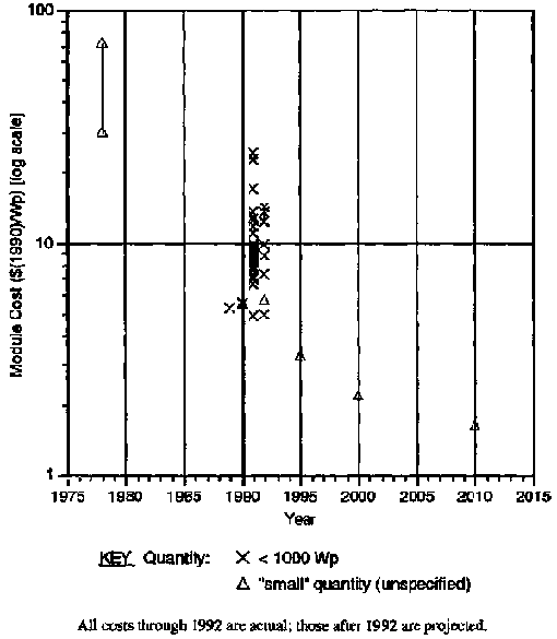
Figure 4.11. Photovoltaic Module
Costs for Small Orders
The following may be deduced from the graphs:
· The costs of
photovoltaic modules have decreased from about $300/Wp (1990 prices) in the
early 1970s to $4 to 11/Wp (1990 prices) in 1992. An outlier figure of over
$1,000/Wp (1990 prices) appears in the early 1970s, which may be due to the
small scale of the application. There are also outlier figures of $2 to 3/Wp
(1990 prices) in 1992; these may be actual production costs.
· The costs vary with the total
quantity (in terms of wattage) required, with larger quantities being cheaper.
· Projections for future cost
reductions show that the cost is expected to drop to $1 to 2/Wp (1990 prices) by
the beginning of the next century. The outliers for 1998 are based on
projections made in the 1980s (Items 114 and 116) and appear optimistic.
· The costs are spread over a
range for both 1991 and 1992. This probably stems from the range of data
collected. This includes both actual module prices in a developing country,
Zimbabwe, as well as actual module prices in the United States (from Real Goods,
a commercial publication). On the other hand, the costs quoted by Zweibel and
Barnett (1993; items 264-66) appear to be actual manufacturing costs.
Furthermore, the latter are for thin-film PV modules, whereas the former are for
crystalline silicon PV modules (except for item 42), which have a higher
manufacturing cost.

Figure 4.12. Photovoltaic Module
Costs for Large Orders

Figure 4.13. Photovoltaic Module
Costs for Unspecified Order Sizes
All costs through 1992 - are actual:; those after 1992 are
projected.
From Figure 4.10, it appears that module costs are expected to
drop further with time. Indeed, as noted earlier, a number of authorities quote
decreases in price with respect to market size (i.e., values for module costs
have been projected for a particular market size). This illustrates the extent
to which economies of scale and the gain in manufacturing experience are
expected to play a part in reducing future costs. Indeed, the "learning curve"
for photovoltaics has been calculated by several authorities (Cody and Tiedje
1992; and Tsuchiya 1992). This is a measure of the decrease in price with
increasing production because of economies of scale and technological progress
and is defined by the following relationship:
 or
or 
where Y = Unit production cost for accumulated production X
X = Accumulated production
a = Cost of a unit at
first production
b = Learning parameter (a negative number)
From this equation, a doubling in the accumulated production
leads to a reduction in the unit cost by a factor, called the progress ratio,
which is usually expressed as a percentage.
Cody and Tiedje (1992) found their data to yield a "77 percent
learning curve" for "silicon solar cells" between 1976 and 1988; that is, that a
doubling of production resulted in costs decreasing to 77 percent of their
initial level. Cody and Tiedje (1992) also report Maycock as identifying a
learning curve parameter as 90 percent for silicon solar cells up to 1965 and 80
percent between 1965 and 1973. Interestingly, Tsuchiya ( 1992) found a similar
result for Japanese photovoltaic production between 1979 and 1988 (i.e., a
nearly "80 percent learning curve"). although he does not specify the type of
photovoltaic module.
These reductions in costs may be attributed to several factors:
· The steady
progress in the efficiency of cells and modules as noted earlier. For example,
efficiencies of crystalline silicon modules have increased by 50 percent from
1976 to 1992; that is, from 7 to 8 percent to 10 to 13 percent. Furthermore, as
discussed earlier, further gains in efficiency are still possible and likely.
· Increases in the scale of
manufacturing, and with this changes in cell design and manufacturing
technologies. The 60-fold increase in the market from 1976, albeit from very
small levels has permitted manufacturers to introduce methods more amenable to
large-scale, low-cost production. Examples are the introduction of thin-film
modules that are amenable to automated manufacturing processes, and the
innovative methods being used for the production of single-crystal silicon
wafers, such as the dendritic web approach which minimize silicon
waste.
Balance-of-system costs
As described earlier, the term balance-of-system can include
supporting structure, power conditioners (to convert the DC power to AC
current); control devices; electrical wiring; batteries for storage; site
preparation; installation; and the secondary system, such as lights or a water
pump. Sources differ in their definition of what exactly constitutes the
balanceof-system, and these inconsistencies make it difficult to compare BOS
costs directly, unless the costs of the individual components are given. These
BOS costs can account for approximately 40 to 60 percent of the total capital
cost according to varying sources. Annex 8 does give an indication of costs of
certain BOS items. These are specified either a percentage of the total cost, or
a total area-related ($/sq. m.) and a total power-related ($/kW) cost, or as
individual component costs. The following should be noted with regard to these
costs:
· The BOS differs in
different applications, from photovoltaics for water pumping to photovoltaics
for generating electricity. Second, further variance is found between a
grid-attached PV system and an individual unit for a house, both producing
electricity. The situation can then become more complicated: Hankins (1993)
gives a number of examples of PV power in developing country situations, where
the system is only required to deliver DC electricity, unlike, say, for a home
in the United States thus eliminating the need for power converters.
· The BOS component parts are
usually made or obtained locally, and thus even further variation is found in
the cost of individual components depending on the site of the PV scheme. See,
for exarnple, items 49 and 50 which compare costs between the Dominican Republic
and the United States (U.S. Congress 1992).
Battery cost is $1,050/kW (lasts 3 to 5 years) in the former,
and $1,400/kW (lasts 3 to 5 years) in the latter. Similarly. the cost of
electronic control equipment is $1,000/kW in the Dominican Republic and
$1,800/kW in the United States. In addition, mounting hardware, with a cost of
$800/kW, is required in the latter, unlike the former
· The cost of the
land and the cost of labor for installation of the PV scheme are again very much
dependent on the site.
· Batteries can make up a large
part of the cost. Variation in cost will be found depending on whether these are
needed for a particular application. An example of an application that may not
require batteries is a utility-based, grid-attached PV plant supplying only peak
power.
Significant reductions in future BOS costs are expected with
increases in:
Module efficiency; this is with regard to area-related BOS
costs, which will decrease as the area requirement is reduced with increasing
module efficiency.
· Market size, which
lead to scale economies.
Table 4.2 shows U.S. DOE ((1992c) and SERI (1989) assessments.
The main reductions are expected to be in power conditioning, wiring and labor
{installation) costs. Increases in inverter and battery life are also projected.

Table 4.2. Balance-of-System Costs
for Photovoltaic
Systems
Cost of photovoltaic electricity
Figures 4.14 and 4.15 show the cost of photovoltaic electricity
as calculated by a variety of different sources taken from the table in Annex 8.
The costs have all been converted to 1990 dollars per kilowatt hour using the
procedure described in Annex 1. Figure 4.14 distinguishes between cases where
the details are given in the reference on the calculative assumptions made; and
Figure 4.15 shows the same data but distinguishes between on-grid and off-grid
generation, as specified by the reference. It is assumed that costs quoted up to
and including 1992 are based on actual component prices, lifetimes, and
efficiencies; though this is not always specified in the text. Costs beyond 1992
are based on projected component costs, lifetimes, and so on, and in some cases
the basis for these projected values is given in the text.
The graphs show that the cost of electricity is decreasing.
However, it is difficult to arrive at conclusions about the rate of decrease,
because different assumptions have been made by different sources for their
calculations. These range from different insolation values, to different
interest rates, to different types and size of schemes; furthermore, because
scale economies are significant, projected costs are particularly dependent on
the scale of the markets assumed. Nevertheless, some trends can be seen. The
figures below compare the cost of photovoltaic electricity (in the same units)
as quoted by different authorities. Current estimates for PV electricity
generation range from 25 to 300 cents (1990)/kWh. Figure 4.15 illustrates the
lower cost of on-grid PV electricity generation compared with remote systems.
This Is partly because of economies of scale (as illustrated earlier by the
lower cost of modules for large quantities) and may also be because storage
costs (i.e., batteries) were not included for on-grid generation. Current cost
estimates for off-grid generation are in the range 25 to 250 cents (1990)/kWh,
whereas those for on-grid generation (where specified as such) are in the range
30 to 40 cents (1990)/kWh.

Figure 4.14. Cost of Electricity from
Photovoltaics
As described earlier in this section, the cost of electricity
depends on several factors, such as insolation, system efficiency, lifetime,
capital costs, O&M costs, and interest rates. The method for calculating the
levelized cost of electricity is shown below:
Cost of electricity (levelized) =  (in $/kWh)
where AC = Annualized capital cost ($/yr)
C =
Total capital cost ($)
A= The annuity
 ,
,
where r=0.01,i.e. a discount rate of 10%, and n =
life of plant (yr)
(O&M) = Annual operating and maintenance cost
($/yr)
E = Number of kilowatt hours produced annually (kWh/yr)

Figure 4.15. Cost of Electricity from
Photovoltaics (Remote and Grid-Attached Generation)
In the case of photovoltaics, the fuel cost is zero. The term
(AC/E) can be written as the sum of three terms: MOD (PV module component) +
BOS(A) (area-related balance-of-system component} + BOS(P) (power-related
balance-of-system component), where


Insol. where
nM = module life (years)
nA
= life of area-related balance of system components (years)
np =
life of power-related balance of system components (years)
CM =
module cost ($/kW)
CA = cost of area-related balance of system
components ($/m2)
Cp = cost of power-related balance of
system components ($/kW)
EffM = module efficiency
(%)
Effs = system efficiency (%) = EffBos x
EffM
EffBOS - balance-of-system efficiency (%)
Insol. = Annual
solar insolation at site (kWh/m2).
As can be seen, longer component lifetimes, higher insolation,
and lower component costs all result in lowering the cost of electricity
generation. It is interesting to see the part played by the module efficiency..
As discussed earlier, the system efficiency is about 70 to 85 percent of the
module efficiency. Thus, in the module component term, MOD, it is only the ratio
of the two (EffM/EffS} that is of importance as the quoted module cost in $/Wp
already accounts for the module efficiency.. The power-related balance-of-system
components, BOS(P), are a function of capacity requirements and being
"downstream" cf the system are not affected by module efficiency.. However, the
area-related balance-of-system, BOS(A), is affected by both module efficiency,
EffM, and system efficiency, Effs. First, the system efficiency is of importance
in determining the electricity generated. Second, the area-related balance of
system costs are linked to the module area and therefore the module efficiency
far a required peak
wattage.
The future of photovoltaics
There is no doubt that costs of photovoltaic modules have
decreased by a factor of 10 over the past 15 years or so and a factor of over 50
since the early 1970s. This decrease has been as a result of both technological
progress and gain in PV production experience. There has also been an increase
in PV module efficiencies. The "bottom line" is the cost of electricity. This
too has decreased, as a result of lower module costs and higher module
efficiencies. Indeed, it is already competitive with the cost of electricity
from conventional technologies in certain instances. Remote sitings are the main
example of this, particularly for small loads, due to the high costs of grid
extension. For example, Waddle and Perlack (1991) found that in Guatemala, PV
systems were less expensive than grid extension when loads were less than 15 to
25 kWh/day and the distance to the nearest tie-point was 6 to 10 km.
The extent of interest and technological research in the field
of photovoltaics appears to offer prospects for further cost reductions, in
particular with the large-scale commercialization of heterojunctional thin-film
modules and multijunctional PV modules, as well as with advances in PV
concentrator technology. Increases in the PV market will also play an important
part in cost reduction because of scale economies and in the creation of
incentives for further technical innovation in manufacturing. The incentive to
PV manufacturers to decrease costs substantially will occur only if the market
increases are large enough to enable the industry to recoup its investment in PV
research and development. Other future issues of importance in the photovoltaic
industry are the supply of raw materials, as the crystalline silicon PV market
expands beyond the "waste" silicon available from the semiconductor industry.
The emphasis to date, however, has been on photovoltaic modules,
when the balance-ofsystem components form 40 to 60 percent of the total cost.
Economies of scale and extensions in component lifetimes are expected to be the
main two factors in reducing these costs further. Batteries, especially, are
mentioned as being a particularly expensive component because of their short
lifetime (3 to 5 years) and consequent need for regular replacement. This,
however, is mainly an issue for remote systems; grid-attached PV systems for the
provision of peak power (if peak insolation and peak demand match) or PV schemes
used in conjunction with an existing hydro scheme have less need for
storage.